nature.com webcasts - Join the discussion, view live or watch on demand

Take our survey for a chance to win a MacBook Air

We'd like to invite you to take part in our annual reader survey. As a thank you for your participation you will have the opportunity to enter a prize draw to win a MacBook Air.

Find out more Remove

Article preview View full access options

Air-stable n-type colloidal quantum dot solids

Journal name:
Nature Materials
Year published:
DOI:
doi:10.1038/nmat4007
Received
Accepted
Published online

Abstract

Colloidal quantum dots (CQDs) offer promise in flexible electronics, light sensing and energy conversion. These applications rely on rectifying junctions that require the creation of high-quality CQD solids that are controllably n-type (electron-rich) or p-type (hole-rich). Unfortunately, n-type semiconductors made using soft matter are notoriously prone to oxidation within minutes of air exposure. Here we report high-performance, air-stable n-type CQD solids. Using density functional theory we identify inorganic passivants that bind strongly to the CQD surface and repel oxidative attack. A materials processing strategy that wards off strong protic attack by polar solvents enabled the synthesis of an air-stable n-type PbS CQD solid. This material was used to build an air-processed inverted quantum junction device, which shows the highest current density from any CQD solar cell and a solar power conversion efficiency as high as 8%. We also feature the n-type CQD solid in the rapid, sensitive, and specific detection of atmospheric NO2. This work paves the way for new families of electronic devices that leverage air-stable quantum-tuned materials.

At a glance

Figures

left
  1. Surface engineering of CQD solids for air stability.
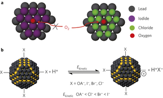
    Figure 1: Surface engineering of CQD solids for air stability.

    a, To realize air-stable n-type CQDs, we sought to prevent the oxidation of the electron-rich n-type CQDs. A complete and robust ligand shell would protect the surface against attack by oxygen. We selected ligands that completely passivate the dangling bonds on the CQD surface, and at the same time sterically inhibit oxidative attack. b, The kinetic energy (Ekinetic) of desorption of different ligands under the attack of hydrogen protons. Yellow and black spheres represent sulphur and lead atoms, respectively. To prevent desorption of halide ligands during ligand exchange, strong binding of the halides is important. Based on density functional theory simulations, the reaction kinetic energy for desorption of iodide is much higher than for chloride. OA, oleic acid.

  2. Halide ligands incorporated in solution-phase and solid-state ligand exchanges.
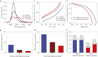
    Figure 2: Halide ligands incorporated in solution-phase and solid-state ligand exchanges.

    a, Photoluminescence spectra of the CQDs after solution–state halide ligands exchange. Iodide-processed CQDs show a sharp exciton emission peak, whereas bromide and chloride show side peaks in the long-wavelength region. Furthermore, the absorbance exciton peak of the chloride-treated sample is broader (Supplementary Fig. 3), also indicating the loss of ligands and the formation of defects. b, Atomic halide to lead ratio of the CQDs after solution–state ligand exchange. The amount of iodide ligands is much higher than chloride and bromide ligands. c, Defect state densities of the CQD films with different halides after solid-state ligand exchange, derived from open-circuit voltage transient decay measurements. EF is the Fermi energy level. The defect state density in the iodide-processed film is much smaller than for films processed with chloride and bromide. d, Halide ligand to lead atomic ratio within the CQD films after the solid-state ligand exchange. Similarly to the solution–state ligand exchange, the amount of iodide ligands is much higher than chloride and bromide. e, Current–voltage curves of the device prepared by post-iodide solution-treated CQD (Method 1 in Supplementary Fig. 7). After air exposure, the open-circuit voltage and power-conversion efficiency of the device are noticeably decreased. Supplementary Table 2 shows the device performance data. f, Effect of halide treatment time on the photoluminescence quantum yield (PLQY) of the CQDs. The PLQY of the original CQDs before any treatment is 30%. CQDs with iodide treatment before methanol washing maintain a PLQY of 30%. However, for the methanol-treated CQDs before iodide treatment, the PLQY decreased to 12%. The post-iodine solution treatment after methanol washing increased the PLQY to 20%45.

  3. Air-stable CQD solar cells.
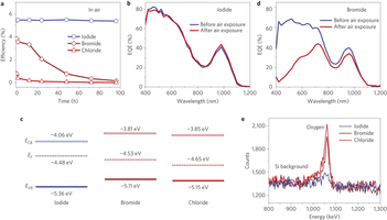
    Figure 3: Air-stable CQD solar cells.

    a, Efficiency of conventional quantum junction devices tested in air and followed over four days (~100 h). Iodide solid-state ligand-exchanged devices show no obvious performance change. For bromide and chloride, the device performance was significantly reduced after air exposure. Details of changes in the parameters for iodide-treated and bromide-treated films are shown in Supplementary Figs 8 and 12, respectively. b, External quantum efficiency (EQE) spectra of a representative iodide solid-state ligand-exchanged device. No change in the spectral shape was observed before and after air exposure. c, Summary of the ultraviolet photoelectron spectroscopy results: Fermi level (EF) and valence band level (EV B) of CQD films with different halide treatments. The conduction band level (ECB) is calculated based on the valence band level and the CQD bandgap. All films were exposed to air before measurements. Iodide-treated films maintain their n-type character, whereas bromide-treated and chloride-treated films become p-type following air exposure. d, EQE spectra of the bromide solid-state-exchanged device before and after air exposure. After air exposure, the EQE value in the blue region is significantly reduced, indicating loss of the junction at the interface between the p-type and original n-type CQD layers. The results suggested that the bromide-processed n-type film was easily oxidized and converted to p-type. e, Rutherford backscattering spectrometry results revealing the oxide content in the film following air exposure for four days. The amounts of oxide in the bromide and chloride solid-state-exchanged film are significantly higher than for iodide, confirming the film is readily oxidized when passivated with chloride and bromide ligands.

  4. Inverted quantum junction devices leverage process-compatible n- and p-type CQD solids.
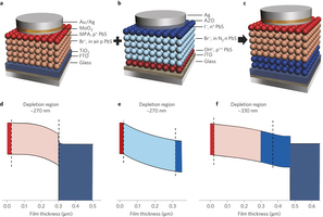
    Figure 4: Inverted quantum junction devices leverage process-compatible n- and p-type CQD solids.

    ac, Schematics of heterojunction (a), conventional quantum junction (b) and inverted quantum junction (c) devices. Mercaptopropionic acid (MPA), bromide (Br-), iodide (I-) and hydroxide (OH-) are the ligands used for the solid-state ligand exchange in film fabrication. The inverted quantum junction device is fabricated by combining the best p-type film in the heterojunction device and the best n-type film in the quantum junction device. df, Simulated spatial band diagrams of the heterojunction (d), quantum junction (e) and inverted quantum junction (f) devices, operating at the maximum power point. The colours in df correspond to those of the layers used in ac. The dashed lines represent the interface between adjacent layers. The depletion region of the CQD layers in the heterojunction and conventional quantum junction devices is ~270 nm. The junction and depletion region in the inverted quantum junction device is located at the interface between the n-type and p-type CQDs, and can be as large as 330 nm.

  5. Inverted quantum junction solar cell.
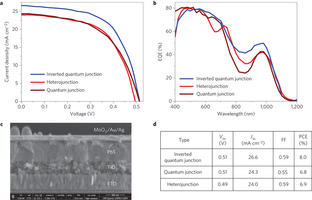
    Figure 5: Inverted quantum junction solar cell.

    a, Current–voltage curves of heterojunction, quantum junction and inverted quantum junction devices. The active layer thickness of all devices is ~450 nm. The inverted quantum junction device shows a much higher current than both the heterojunction and quantum junction devices. b, EQE spectra of all three devices. The inverted quantum junction device shows appreciably higher EQE values in the infrared region, which can be ascribed to its large depletion region. c, SEM cross-section image of the inverted quantum junction device, with an active layer thickness of ~450 nm (scale bar, 500 nm). d, Open-circuit voltage (Voc), short-circuit density (Jsc), fill factor (FF) and power-conversion efficiency (PCE) for inverted quantum junction, quantum junction and heterojunction photovoltaic devices.

right

References

  1. Shirasaki, Y., Supran, G. J., Bawendi, M. G. & Bulovic, V. Emergence of colloidal quantum-dot light-emitting technologies. Nature Photon. 7, 1323 (2013).
  2. Sun, L. et al. Bright infrared quantum-dot light-emitting diodes through inter-dot spacing control. Nature Nanotech. 7, 369373 (2012).
  3. Tang, J. et al. Colloidal-quantum-dot photovoltaics using atomic-ligand passivation. Nature Mater. 10, 765771 (2011).
  4. Wang, X. et al. Tandem colloidal quantum dot solar cells employing a graded recombination layer. Nature Photon. 5, 480484 (2011).
  5. Luther, J. M. et al. Schottky solar cells based on colloidal nanocrystal films. Nano Lett. 8, 34883492 (2008).
  6. Brown, P. R. et al. Improved current extraction from ZnO/PbS quantum dot heterojunction photovoltaics using a MoO3 interfacial layer. Nano Lett. 11, 29552961 (2011).
  7. Ma, W. et al. Photovoltaic performance of ultrasmall PbSe quantum dots. ACS Nano 5, 81408147 (2011).
  8. Konstantatos, G. et al. Ultrasensitive solution-cast quantum dot photodetectors. Nature 442, 180183 (2006).
  9. David, K. K., Lai, Y., Diroll, B. T., Murray, C. B. & Kagan, C. R. Flexible and low-voltage integrated circuits constructed from high-performance nanocrystal transistors. Nature Commun. 3, 1216 (2012).
  10. Lee, J. S., Kovalenko, M. V., Huang, J., Chung, D. S. & Talapin, D. V. Band-like transport, high electron mobility and high photoconductivity in all-inorganic nanocrystal arrays. Nature Nanotech. 6, 348352 (2011).
  11. Choi, J. H. et al. Bandlike transport in strongly coupled and doped quantum dot solids: A route to high-performance thin-film electronics. Nano Lett. 12, 26312638 (2012).
  12. Choi, J. H. et al. In-situ repair of high-performance, flexible nanocrystal electronics for large-area fabrication and operation in air. ACS Nano 7, 82758283 (2013).
  13. Sargent, E. H. Colloidal quantum dot solar cells. Nature Photon. 6, 133135 (2012).
  14. Johnston, K. W. et al. Schottky-quantum dot photovoltaics for efficient infrared power conversion. Appl. Phys. Lett. 92, 151115 (2008).
  15. Pattantyus-Abraham, A. G. et al. Depleted-heterojunction colloidal quantum dot solar cells. ACS Nano 4, 33743380 (2010).
  16. Engel, J. H., Surendranath, Y. & Alivisatos, A. P. Controlled chemical doping of semiconductor nanocrystals using redox buffers. J. Am. Chem. Soc. 134, 1320013203 (2012).
  17. Chang, L-Y., Lunt, R. R., Brown, P. R., Bulović, V. & Bawendi, M. G. Low-temperature solution-processed solar cells based on PbS colloidal quantum dot/CdS heterojunctions. Nano Lett. 13, 994999 (2013).
  18. Osedach, T. P. et al. Bias-stress effect in 1, 2-ethanedithiol-treated PbS quantum dot field-effect transistors. ACS Nano 6, 31213127 (2012).
  19. Zhao, N. et al. Colloidal PbS quantum dot solar cells with high fill factor. ACS Nano 4, 37433752 (2010).
  20. Jean, J. et al. ZnO Nanowire arrays for enhanced photocurrent in PbS quantum dot solar cells. Adv. Mater. 25, 27902796 (2013).
  21. Strasfeld, D. B., Dorn, A., Wanger, D. D. & Bawendi, M. G. Imaging Schottky barriers and ohmic contacts in PbS quantum dot devices. Nano Lett. 12, 569575 (2012).
  22. Luther, J. M. & Pietryga, J. M. Stoichiometry control in quantum dots: A viable analog to impurity doping of bulk materials. ACS Nano 7, 18451849 (2013).
  23. Lan, X. et al. Self-assembled, nanowire network electrodes for depleted bulk heterojunction solar cells. Adv. Mater. 25, 17691773 (2013).
  24. Luther, J. M. et al. Stability assessment on a 3% bilayer PbS/ZnO quantum dot heterojunction solar cell. Adv. Mater. 22, 37043707 (2013).
  25. Nozik, A. J. et al. Semiconductor quantum dots and quantum dot arrays and applications of multiple exciton generation to third-generation photovoltaic solar cells. Chem. Rev. 110, 68736890 (2010).
  26. Scheele, M. et al. Nonmonotonic size dependence in the hole mobility of methoxide-stabilized PbSe quantum dot solids. ACS Nano 7, 67746781 (2013).
  27. Ma, W., Luther, J. M., Zheng, H., Wu, Y. & Alivisatos, A. P. Photovoltaic devices employing ternary PbSxSe1−x nanocrystals. Nano Lett. 9, 16991703 (2009).
  28. Engel, J. & Alivisatos, A. P. Postsynthetic doping control of nanocrystal thin films: Balancing space charge to improve photovoltaic efficiency. Chem. Mater. 26, 153162 (2014).
  29. Ning, Z. et al. Wave-function engineering of CdSe/CdS Core/Shell quantum dots for enhanced electron transfer to a TiO2 Substrate. J. Phys. Chem. C 114, 1518415189 (2010).
  30. Ip, A. H. et al. Hybrid passivated colloidal quantum dot solids. Nature Nanotech. 7, 577582 (2012).
  31. Research Cell Efficiency Records by National Renewable Energy Laboratory, version at November 2013. http://www.nrel.gov/ncpv/images/efficiency_chart.jpg
  32. Zhitomirsky, D. et al. N-type colloidal-quantum-dot solids for photovoltaics. Adv. Mater. 24, 61816185 (2012).
  33. Tang, J. et al. Quantum junction solar cells. Nano Lett. 12, 48894894 (2012).
  34. Ning, Z. et al. Graded doping for enhanced colloidal quantum dot photovoltaics. Adv. Mater. 25, 17191723 (2013).
  35. Wei, P., Oh, J. H., Dong, G. F. & Bao, Z. Use of a 1H-benzoimidazole derivative as an n-type dopant and to enable air-stable solution-processed n-channel organic thin-film transistors. J. Am. Chem. Soc. 132, 88528853 (2010).
  36. Liu, Y. PbSe Quantum dot field-effect transistors with air-stable electron mobilities above 7 cm2 V−1 s−1. Nano Lett. 13, 15781587 (2013).
  37. Shim, M. & Guyot-Sionnest, P. n-type colloidal semiconductor nanocrystals. Nature 407, 981983 (2000).
  38. Talapin, D. V. & Murray, C. B. PbSe nanocrystal solids for n- and p-channel thin film field-effect transistors. Science 310, 8689 (2005).
  39. Mocatta, D. et al. Heavily doped semiconductor nanocrystal quantum dots. Science 332, 7781 (2011).
  40. Koh, W-k. et al. Heavily doped n-type PbSe and PbS nanocrystals using ground-state charge transfer from cobaltocene. Sci. Rep. 3, 2004 (2013).
  41. Voznyy, O. et al. Charge-orbital balance picture of doping in colloidal quantum dot solids. ACS Nano 6, 84488455 (2012).
  42. Hassinen, A. et al. Short-chain alcohols strip X-type ligands and quench the luminescence of PbSe and CdSe quantum dots, acetonitrile does not. J. Am. Chem. Soc. 134, 2070520712 (2012).
  43. Vande Vondele, J. et al. Quickstep: Fast and accurate density functional calculations using a mixed Gaussian and plane waves approach. Comput. Phys. Commun. 167, 103128 (2005).
  44. Pearson, R. G. Hard and soft acids and bases. J. Am. Chem. Soc. 85, 35333539 (1963).
  45. Ning, Z. et al. All-inorganic colloidal quantum dot photovoltaics employing solution-phase halide passivation. Adv. Mater. 24, 62956299 (2012).
  46. Burgelman, M., Nollet, P. & Degrave, S. Modelling polycrystalline semiconductor solar cells. Thin Solid Films 361–362, 527532 (2000).
  47. Liu, H. et al. Tin oxide films for nitrogen dioxide gas detection at low temperatures. Sens. Actuat. B 177, 460466 (2013).
  48. Barkhouse, D. A. R. et al. Depleted bulk heterojunction colloidal quantum dot photovoltaics. Adv. Mater. 23, 31343138 (2011).
  49. Liu, H. et al. Systematic optimization of quantum junction colloidal quantum dot solar cells. Appl. Phys. Lett. 101, 151112 (2012).
  50. Liu, H. et al. Electron acceptor materials engineering in colloidal quantum dot solar cells. Adv. Mater. 23, 38323837 (2011).

Download references

Author information

Affiliations

  1. Department of Electrical and Computer Engineering, University of Toronto, 10 King’s College Road Toronto, Ontario, M5S 3G4, Canada

    • Zhijun Ning,
    • Oleksandr Voznyy,
    • Sjoerd Hoogland,
    • Valerio Adinolfi,
    • Jixian Xu,
    • James Minor,
    • Kyle W. Kemp,
    • Haopeng Dong,
    • Lisa Rollny,
    • André Labelle,
    • Graham Carey,
    • Brandon Sutherland &
    • Edward H. Sargent
  2. Division of Physical Sciences and Engineering, Solar and Photovoltaics Engineering Center, King Abdullah University of Science and Technology (KAUST), Thuwal 23955-6900, Saudi Arabia

    • Jun Pan,
    • Ahmad R. Kirmani,
    • Aram Amassian &
    • Osman M. Bakr
  3. School of Optical and Electronic Information, Huazhong University of Science and Technology, 1037 Luoyu Road Wuhan, Hubei 430074, China

    • Min Li &
    • Huan Liu
  4. Dalhousie University, Department of Physics and Atmospheric Science, Rm 319 Dunn Building Halifax, Nova Scotia, B3H 4R2, Canada

    • Jon-Paul Sun &
    • Ian Hill
  5. Wuhan National Laboratory for Optoelectronics, Huazhong University of Sciences and Technology, 1037 Luoyu Road Wuhan, Hubei 430074, China

    • Jiang Tang

Contributions

Z.N., O.V., O.M.B. and E.H.S. designed and directed this study, analysed the results, and co-wrote the manuscript. Z.N. contributed to all experimental work. O.V. carried out the density functional theory simulations and XPS measurements. J.P, J.X. and H.D. assisted in device fabrication. S.H. and J.M. performed transient photovoltage experiments. V.A carried out optoelectronic simulations. M.L., H.L. and J.T. performed NO2 gas sensing measurements. K.W.K., L.R., A.L., G.C. and B.S. carried out fabrication and device characterization of specific devices. A.R.K. and A.A. performed UPS measurement. J-P.S. and I.H. carried out the Kelvin probe study.

Competing financial interests

The authors declare no competing financial interests.

Corresponding author

Correspondence to:

Author details

Supplementary information

PDF files

  1. Supplementary Information (1,039 KB)

    Supplementary Information

Additional data